Apple’s Supply Chain: TSMC at the Core:- In the world of smartphones, Apple’s iPhone reigns supreme, in the 2023 fiscal year, Apple reported a net income of $96.99 billion and total revenues of $383 billion. Apple Inc is Taiwan Semiconductor Manufacturing Company (TSMC)’s largest customer, accounting for 23% of the company’s $72 billion revenue in 2022. A significant factor contributing to Apple’s success is its reliance on TSMC for semiconductor chip production.
Why does Apple Depends on TSMC? TSMC is a critical partner for Apple due to its unmatched ability to manufacture the world’s most advanced, smallest, and highest-performing transistors. Transistors, the building blocks of logic gates, combine to form arithmetic logic units (ALUs), control units, and other processing elements in CPUs. Scaling transistors increases memory capacity without expanding physical size. This aligns with Moore’s law, which states, “The number of transistors on a microchip doubles approximately every two years, leading to an exponential increase in computing power and a decrease in relative cost.” TSMC’s 3nm process can accommodate up to 250 million transistors per square millimeter, compared to 170 million transistors in the 5nm node, depending on the design. This technology delivers 25-30% power savings over 5nm, making it vital for mobile devices, data centers, and energy-efficient applications. Apple has secured the entire supply of TSMC’s 3nm technology for its iPhone 15 Pro and M3 Macs. In 2024, at the Open Innovation Platform (OIP) event in the Netherlands, TSMC announced plans to introduce the A16 chip, built on the 1.6nm fabrication process, by 2026. These cutting-edge chips are essential for powering Apple’s devices, enabling superior performance, energy efficiency, and technological innovation across its product lineup. Hence, TSMC’s capability to manufacture the smallest and highest-performing chips is crucial to Apple’s success.
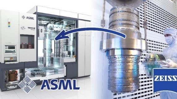
Apple procures advanced semiconductor chips from TSMC, which, in turn, sources DUV and EUV lithography machines from Advanced Semiconductor Materials Lithography (ASML). ASML relies on Zeiss SMT for the critical component of its lithography systems, known as the Light Module or Light Engine. This is the heart of semiconductor optical lithography equipment! The Light Module is an intricate assembly of optical elements engineered with sub-nanometer surface roughness and exceptional alignment precision. This system enables the projection of structures smaller than the diffraction limit of the laser wavelength.
In early photolithography, mercury vapor lamps were the primary light sources, emitting ultraviolet (UV) light at specific wavelengths, notably the i-line (365 nm) and h-line (405 nm). These lamps provided stable and intense UV radiation suitable for patterning micro- and nanostructures. Photolithography involved placing a photomask (mask based lithography) with the desired pattern between the UV source and a substrate coated with a photosensitive resist. Patterns were transferred using contact printing, proximity printing, or projection lenses, with resolution constrained by diffraction limits, typically achieving feature sizes around 500 nm. So, what is the technology which makes TSMC to produce a node below 10nm?
The smallest size of transistor which can be printed in photolithography is directly linked to the wavelength of light used; shorter wavelengths enable smaller feature sizes. ASML’s Deep Ultraviolet (DUV) lithography utilizes excimer lasers, notably Krypton Fluoride (KrF) with a wavelength of 248 nm and Argon Fluoride (ArF) with a wavelength of 193 nm. These lasers produce coherent, high-intensity light, which is essential for precise patterning on silicon wafers.
Wavelengths like 193 nm, coupled with advanced techniques such as immersion lithography—where a high-refractive-index liquid is introduced between the lens and the wafer to increase the Numerical Aperture (NA)—enable resolution down to sub-50 nm features. These capabilities make DUV suitable for manufacturing transistors and interconnects in technology nodes such as 45 nm, 28 nm, and even some 14 nm processes. The theoretical resolution limit is described by Rayleigh’s criterion, R=k×(wavelength)/NA where k is a process-dependent factor, typically around 0.61 for imaging applications. By manipulating light and employing innovative techniques, k can be reduced to as low as 0.25, enabling feature sizes smaller than the nominal diffraction limit. For instance, the 45 nm node was achieved with k≈0.31. The nodes achieved below 45nm utilizes advancements in material chemistry and novel process technologies like multiple patterning to overcome conventional resolution. The use of multiple patterning techniques with DUV lithography and how EUV lithography eliminates the need for such methods to achieve the smallest technology nodes will be addressed in a subsequent article.
Now, we will understand how to achieve the value of k=0.31? Achieving a low k-value is essential for producing finer features in advanced lithography. Techniques like direct-write lithography, such as Electron Beam Lithography (EBL), are capable of producing the smallest features like below 10nm due to its smallest less than nanometer scale wavelength. However, the throughput (the number of wafers processed per unit of time) of EBL is extremely low, as the process involves writing patterns sequentially on a wafer, making it impractical for large-scale transistor production. For high-volume manufacturing, mask-based lithography is used, which enables the replication of tens of thousands of identical patterns from a single mask, akin to injection molding in toy manufacturing. While creating the initial mold (or mask) requires significant time and cost, replication is rapid and cost-effective.
To understand how k-values are reduced, consider the scenario of transferring a grating pattern (closely spaced lines) onto a wafer as in schematic Figure1. When a light beam of 1 mm diameter is directed onto the grating, it creates diffraction spots of various orders. For the pattern to be accurately transferred, the lens below the mask must capture the first diffraction orders. As the spacing between grating lines decreases, the diffraction angles increase, requiring larger lenses to capture the diffracted beams. An alternative approach to accommodate smaller features is to increase the beam diameter (e.g., from 1 mm to 1 cm). This adjustment ensures that the zeroth and first-order diffraction spots interfere at the lens edges, effectively reducing the k-value to 0.25.

However, a larger beam diameter reduces image contrast, as the central part of the lens transmits uniform light without sufficient interference. To address this, beam shaping is employed. By blocking the center of the beam and allowing only the outer edges (creating an annular or ring-shaped beam) to expose the mask, the contrast on the wafer improves. Further refinement involves off-axis illumination techniques, such as dipole illumination (where only two opposite edges of the beam are exposed) or quadrupole illumination (where four edges are used).
In present mask-based lithography, the mask is scanned in the x- and y-directions while the shaped beam continuously exposes it. The scanning and printing process is extremely fast, enabling machines like the ASML Oil Immersion DUV TWINSCAN NXT:1470 to print up to 300 wafers of 300 mm diameter per hour. This translates to printing one wafer every 12 seconds. For perspective, consider the production of modern chips. The Apple M1 chip, built on a 5-nanometer process technology, contains 16 billion transistors within an area of 119 mm². With the speed of advanced lithography machines, 40–50 M1 chips can be fabricated every second, demonstrating the remarkable efficiency of modern lithographic processes.
Projection Optics and Reduction optics in lithography: Most masks for DUV and EUV lithography are fabricated using electron beam lithography (EBL) due to its precision in creating intricate patterns. These masks are used in projection lithography, where patterns from the mask are projected onto the wafer, unlike the earlier contact lithography methods. In projection lithography, the mask does not come into direct contact with the photoresist like contact lithography, preserving the mask from damage and enabling multiple reuse.
A key advantage of projection lithography is its capability for reduction lithography, which reduces the image size of the mask. Typically, reduction ratios are 4:1 or 5:1, meaning a mask feature of 200 nm can produce a 50 nm feature on the wafer. The projection system achieves this by directing the first-order diffracted light spots collected from the initial lens through a series of convex and concave lenses. These lens assemblies, which may include 10–20 optical elements, reduce the pattern size and correct optical aberrations such as spherical aberration, astigmatism, and field curvature, ensuring a sharp and distortion-free image.
For comparison, the best camera systems used for photography or filming maintain a root-mean-square (RMS) aberration of around 200 nm. In contrast, lithography optics must correct aberrations to below 10 nm—20 times more stringent—to achieve the precision required for semiconductor manufacturing. Zeiss, a leader in precision optics, recently stated that it manufactures the most precise mirrors for EUV lithography. To illustrate their precision, if a mirror were scaled to the size of Germany, its surface roughness would be less than 100 microns, approximately the thickness of a human hair. In projection lithography, lenses near the photomask handle collimation and initial focusing, while middle lenses focus and reduce the image. The final lenses project the reduced image onto the wafer with a high numerical aperture (NA) to achieve fine resolution. Zeiss also reported that 80% of all microchips worldwide are produced using its optical systems, underscoring their critical role in modern semiconductor fabrication.
With increase in NA and decrease in wavelength (using EUV) transistors have approached atomic scales, leading to challenges like quantum tunnelling and heat dissipation and the cost of developing and manufacturing smaller transistors has increased significantly. ASML builds the skeleton and body mass of the lithography system, much like the framework of a human body, while Zeiss creates the heart—the light module—that powers the system by delivering precision lens, projection system and innovative ideas to further reduce the k value. TSMC is looking forward to get high NA EUV machine and Apple has an eye on TSMC chips and the role of Optical engineer/Scientist is hidden behind each Apple iphone.
Future topics which I would like cover are
· India’s Semiconductor Quest: Challenges and Delays in Building a Chipmaking Ecosystem
· The Science and Journey of Immersion DUV in Modern Lithography
· EUV Lithography: From Concept to Reality in Advanced Node Manufacturing
· Dissecting Your Smartphone: The Hidden World of Microchips
· Challenges and Opportunities in AR/VR Adoption
Quite insightful article! Looking forward to reading the future topics you will cover.