
When the world tilts toward disaster, there is always one person standing between chaos and survival—the astronaut improvising solutions as a spacecraft loses power, the submarine captain navigating blind through deep-ocean darkness, the wildfire commander predicting how flames will jump before the wind does. These are moments where there is no script, no second chance. That leader must read dozens of signals at once, recall years of experience instantly, connect invisible patterns, and make decisions faster than the danger can unfold. Their brain becomes a living circuit of perception, communication, logic, and intuition firing in perfect synchrony to prevent catastrophe.
This is the same transformation happening inside our machines. Modern AI systems are beginning to think the way crisis-tested humans do—absorbing floods of data, identifying hidden patterns, and acting with precision when milliseconds matter. And behind this new intelligence lies the silicon that powers it all: chips that function like memory, senses, logic, and communication fused into one nervous system. These chips no longer just run devices; they make predictions, guide decisions, and increasingly shape the world just as decisively as those real-world leaders do.
A smartphone, a car, a drone, or any AI-enabled device must sense the world, interpret signals, recall stored knowledge, calculate risks, and act instantly. Its sensors are its eyes and ears. Its memory chips store everything it has learned. Its communications modules bring in live data. Its processors and AI engines turn signals into understanding. Just like a crisis leader, the device must connect the dots under pressure—only far faster than any human could. And that is why AI changed everything.
When models like ChatGPT, Gemini, and Claude began writing software, forecasting cyclones, analyzing proteins, and generating full-length films on NVIDIA’s GPUs, the world finally woke up. Chips weren’t electronic components anymore. They were the engines of human progress. NVIDIA’s processors became the new power plants of civilization—driving biotech, climate science, defense intelligence, autonomous vehicles, and trillion-dollar industries. In July 2025, NVIDIA brushed against a $4 trillion valuation. By October, it shattered economic history by crossing $5 trillion, becoming the most valuable company the world has ever seen.
But Wall Street cheering was the least important part. Behind closed doors, governments panicked. Because if one company’s silicon can accelerate scientific discovery, transform industries, and amplify military capabilities… then whoever controls chip manufacturing controls the future itself.
That realization triggered a global spending race unlike anything the tech world has seen:
– The U.S. unleashed $52B through the CHIPS Act.
– Europe countered with €43B.
– Japan, fighting to reclaim its semiconductor glory, committed over $30B.
– And India—refusing to repeat the mistake of missing the internet boom—deployed more than $10B for its semiconductor mission.
All this money. All this urgency. All for devices smaller than your thumbnail.
Then came the plot twist that sent global anxiety into overdrive: over 90% of the world’s advanced chips are manufactured on one island—Taiwan. Suddenly politicians, CEOs, and military strategists realized that modern civilization hangs on a supply chain that could be disrupted by a typhoon, a blockade, or a political miscalculation.
No chips means no smartphones, no EVs, no aircraft, no hospitals, no payments, no satellites, no AI training clusters. Chips are no longer commodities; they are the new oil, the backbone of national security, and the currency of modern power.
But here’s the twist few people ever realize: the race for AI superchips doesn’t stop in data centers—it spills directly into your smartphone. What sits inside your phone isn’t just engineering. It’s a map of alliances, vulnerabilities, and ambitions—etched into silicon.
A modern smartphone is not one chip—it is 60 to 80 specialized chips and sensors working together like a small electronic civilization. Roughly 15–20 of these belong to processing and graphics tasks, 10–15 handle connectivity, 8–12 manage memory and storage, another 10 monitor power and charging, around 20 are sensors and imaging blocks, and the rest belong to audio, haptics, and security. Each chip originates from a different factory and often a different country, stitched together inside one thin device you carry in your hand. This complexity is why a smartphone is not a product; it is a global alliance of semiconductor companies packed into six inches of glass.
Deep inside this small world, the compute engines act like the thinkers and planners of the city. These include CPUs, GPUs, NPUs, ISPs, and cache controllers—typically 15 to 20 subsystems fused into one SoC. Companies like Qualcomm, MediaTek, Apple, and Samsung design these engines, while TSMC or Samsung fabricate them using 3 nm, 4 nm, or 5 nm nodes. A single SoC may carry a trillion operations per second for AI tasks and up to 10 billion pixels per second for imaging, all while staying under a few watts of power. This category alone determines how fast apps open, how smooth games run, and how intelligent the phone feels, and it is also the part of the phone where the most money, R&D, and marketing battles happen.
If compute engines are the brains, connectivity chips are the voice and ears, usually 10 to 15 chips bundled around a 5G modem. These include RF transceivers, power amplifiers, Wi-Fi 7 modules, Bluetooth controllers, Global Navigation Satellite System (GNSS) receivers, Near Field Communication (NFC) chips, and antenna tuners. Qualcomm and MediaTek dominate modems, while Broadcom, Qorvo, Skyworks, Murata, and Intel contribute Wi-Fi and RF components. A smartphone may switch across 40–60 frequency bands in a single day, and these chips ensure it can talk to cell towers, satellites, earbuds, smartwatches, and routers seamlessly. Without this silent network of silicon diplomats, your phone would be nothing more than a disconnected brick.
Companies like Samsung, SK Hynix, Micron, and Kioxia supply most of the mobile memory used worldwide. Modern NAND flash storage stacks up to 200 layers of memory cells vertically, like a microscopic skyscraper. LPDDR RAM is the phone’s short-term memory. It handles active tasks:
your opened apps, camera preview, game frames, browser tabs, and background processes. UFS storage is the long-term memory. It stores your photos, videos, apps, downloads, OS files, preferences—everything that defines your digital life. RAM today achieves speeds of 4–6 GB/s, while UFS storage crosses 3 GB/s, enabling your smartphone to feel fast and responsive even with many apps running simultaneously.
Just as a city depends on power plants and electricians, a smartphone relies on its power-management ecosystem—typically 8 to 10 specialized chips that quietly keep the device alive. The PMIC (Power Management Integrated Circuit) acts like the central power controller, distributing electricity from the battery to every block of the SoC. Buck converters adjust and regulate voltage levels so each component receives exactly what it needs—no more, no less. Charging ICs manage fast charging, negotiating power levels with chargers that can go up to 200 watts. Fuel-gauge ICs track battery health and accurately estimate how many minutes or hours you have left, down to the millivolt. Companies like Texas Instruments (TI), Qualcomm, NXP, Renesas, and Richtek build the chips that run this silent infrastructure. Without these components working perfectly together, the phone would overheat, drain power too quickly, or charge inconsistently. They are invisible to users—but they ultimately decide whether your phone survives a full day or dies before lunch.
Then come the sensors—the phone’s eyes, ears, skin, and inner ear. A modern flagship smartphone carries 18 to 22 sensors, all working together to understand the world. Camera sensors (built by Sony and Samsung) capture light and form images. These are large, high-precision chips. Companies like Bosch, STMicroelectronics, and TDK supply the motion and environment sensors, such as: Gyroscopes – detect rotation, Accelerometers – detect movement and vibration, Barometers – measure air pressure for altitude, Magnetometers – detect direction like a digital compass, MEMS microphones – tiny microphones built with micro-machined structures. For depth perception, phones use ToF (Time-of-Flight) sensors or LiDAR (Light Detection and Ranging) units from Infineon or Lumentum. These sensors detect light, motion, sound, distance, tilt, pressure, and direction. Together they allow your camera to focus instantly, keep AR (Augmented Reality) objects stable, and help maps track your orientation even when GPS is unavailable. Among all smartphone components, sensors contribute the most to how the outside world enters the digital world.
Finally, the personality of the phone emerges from about 5 to 8 chips responsible for sound, touch, and identity. Audio codecs and amplifiers—typically from Cirrus Logic, Qualcomm, ESS, or NXP—convert digital bits into the music and voice you hear. Haptic drivers from AAC or Qorvo create the tactile feel of keyboard clicks or gaming vibrations. Security chips, like Apple’s Secure Enclave or Qualcomm’s SPU, store fingerprints, encryption keys, and face data in hardware-protected zones. These chips don’t make benchmarks, but they define how intimate, safe, and human the device feels.
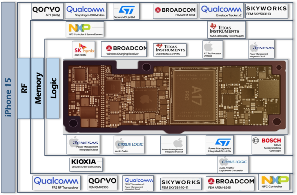
Figure:A glimpse into the iPhone 15’s silicon ecosystem—many more chips, sensors, and companies lie beneath the surface.
As smartphones absorb more responsibilities, humans quietly raise their expectations. We no longer want a device that only calls, texts, and photographs—we want a handheld laboratory. People want to check the air quality around them, volatile chemicals, allergens, and even pollutants specific to their neighborhood. They want to test the purity of drinking water in seconds, measure pesticide residue on vegetables, verify whether food companies are truthful about nutritional composition, and know if fruits are naturally ripened or artificially treated. Farmers want phones that read soil chemistry and moisture levels, detect plant diseases early, and forecast harvest dates with scientific accuracy. Parents want to detect spoiled food, bad milk, gas leaks, or harmful microbes. Students want a microscope in their pocket. Travelers want real-time radiation detection, humidity sensing, altitude accuracy, and UV monitoring. Every one of these instincts points to one direction: people want sensors that normally live inside labs to shrink into a smartphone.
But shrinking laboratory instruments is not like shrinking CPUs from the 1990s. Making an oscilloscope smaller is one thing—miniaturizing mass spectrometers, spectrometers, chemical analyzers, and microscopes is another. Electronics can scale with transistors; physics does not scale as easily. Still, new sensor classes are emerging. Compact spectrometers based on metasurfaces, tunable filters, and tiny interferometers are beginning to measure chemical signatures directly from reflected light. Gas sensors based on graphene or metal-oxide films are detecting molecules at parts-per-billion. Chip-scale microscopes with computational optics are letting phones see bacteria. Thermal and hyperspectral sensors are turning cameras into scientific imagers. These next-generation devices fall into categories that already exist inside phones—optical sensors, chemical sensors, environmental sensors—but their complexity pushes them far beyond traditional MEMS or camera modules. Instead of 20 sensors in a flagship phone, the next era may push that number to 60 or even 100 across all categories.
With every new sensor, computation becomes the bottleneck. A modern spectrometer sensor may produce hundreds of data points per measurement; a hyperspectral camera may capture 50–100 wavelength bands per frame; a chip-based microscope can generate tens of millions of micro-images that must be computationally reconstructed. This is where GPUs—once only for gaming—become the new lungs of smartphones. They breathe life into raw sensor data by converting matrices, spectra, and signals into clean visual information in milliseconds. The sentence people often say—“the key to sensors is GPU”—is directionally right but slightly incomplete. It is not only the GPU; it is the GPU+NPU ecosystem. The GPU handles parallel math for graphics-heavy sensor reconstruction, while the NPU handles AI-driven denoising, classification, detection, segmentation, and prediction. Together they make a raw hyperspectral image look like a simple color photo, or convert the output of a chemical sensor into a clear yes/no answer.
This need for compute is also why NVIDIA rose to the summit of the semiconductor industry. By 2025, NVIDIA became the first company to cross a $5 trillion valuation—larger than any chip company in history—because the world realized that every future device, whether phone, drone, microscope, or robot, needs vast parallel compute to transform data into intelligence. Between 2020 and 2025, NVIDIA’s revenue and market share in GPUs grew explosively due to the AI boom, data centers, and edge computing. Their GPUs became the global standard for both training and inference, and even mobile chip designers began adopting the same architectural principles—massive parallelism, tensor operations, and memory-optimized pipelines. Smartphones don’t use NVIDIA GPUs directly, but they now carry miniature versions inspired by them.
Yet even with all these improvements, a problem remains that no electronic chip can solve alone: certain computations scale beyond what electrons can handle efficiently. Consider weather prediction. A regional model calculating probability for rainfall or cyclone intensities might require tens of trillions of floating-point operations per second for hours. A smartphone GPU performing 2–5 teraflops cannot approach this. Even desktop GPUs struggle. The reason is fundamental: electrons move through copper at about 1–5% of the speed of light, constantly generating heat. As computation needs climb—from analyzing hyperspectral sensor arrays to running real-time climate models or molecular detectors—electronic chips hit a thermal wall.
This is why the world is chasing photonic and quantum chips. Photonic processors use light instead of electrons. Light travels at the speed of light (literally), produces minimal heat, and allows matrix multiplications to be performed almost instantaneously using interference patterns. Tasks that take a modern electronic GPU 1 millisecond could be done in 1 picosecond on a photonic accelerator—one million times faster. Quantum chips, built around qubits, don’t beat GPUs on everyday tasks but dominate problems involving optimization, simulation, cryptography, and molecular modeling. A quantum chip may solve in minutes a problem that would take classical supercomputers thousands of years. These are the engines needed if smartphones are ever to become true portable laboratories able to detect chemicals, simulate biological reactions, or predict environmental changes in real time.
But both technologies face challenges. Photonic chips require perfect alignment, stable lasers, and ultra-precise waveguides—difficult to mass-produce. Quantum processors require cryogenic or error-corrected qubits, far from fitting inside a phone. Yet the world is moving toward hybrid architectures: electronics for control, photonics for acceleration, and quantum for specialized tasks. Just as phones today use CPUs+GPUs+NPUs, future phones may use electronic+photonic+quantum hybrids.
And that is the direction the smartphone is evolving: from a communication tool to a personal scientific instrument. From a camera to a chemical analyzer. From an entertainment device to a miniature AI supercomputer. The number of chips will grow, the categories will expand, and what seems impossible today will quietly become normal—just as cameras, compasses, and accelerometers once did
India’s Rise in the Chip Race: Not by Competing on 3nm, but by Redefining What the Future Chip Looks Like
As the world scrambles to secure the future of chips, India has begun writing a serious new chapter in this global semiconductor race. For decades, the country was only a massive consumer—importing every processor, sensor, and memory chip that powered its billion smartphones. But as India became the second-largest smartphone market and AI began reshaping the global economy, a blunt realization hit policymakers and industry leaders: If chips determine the future, relying entirely on imports means outsourcing your own future.
That realization triggered a shift—not through diplomatic statements, but through industrial partnerships and billion-dollar projects under the India Semiconductor Mission. Tata Electronics stepped forward first, announcing a semiconductor fabrication plant in Gujarat in partnership with Powerchip Semiconductor Manufacturing Corporation (PSMC) of Taiwan. Kaynes Technology secured approval for an advanced OSAT/ATMP facility in Gujarat to handle chip packaging and testing, backed by foreign process expertise. The HCL Group entered a joint venture with Foxconn to establish a fab in Uttar Pradesh—one of the most high-profile India–Taiwan–U.S. linked semiconductor announcements yet. Even state governments began competing: Gujarat building dedicated semiconductor clusters, Tamil Nadu announcing plans for semiconductor parks, and other states racing to attract equipment suppliers and talent.
What makes these moves meaningful is that India is not trying to reinvent the semiconductor wheel from scratch. It is deliberately partnering with global leaders to compress decades of learning into a few years. Applied Materials committed major investment into an R&D center in India. Japanese and American firms offered manufacturing knowledge, design tools, and patented processes. Taiwan contributed long-term manufacturing expertise through structured agreements. Each partnership is a shortcut through time—an attempt to accelerate India’s semiconductor capability by standing on the shoulders of those who’ve built it before.
And behind all this, the government laid down its boldest industrial bet since the IT revolution: over ₹76,000 crore (nearly $10 billion) in semiconductor incentives, offering up to 50% support for fabs and 75% for compound-semiconductor and display projects. Almost the entire fund—97% of it—has already been allocated to approved projects, signaling how aggressively India is pushing to secure its place in the global chip supply chain.
India is not claiming leadership yet. But for the first time in history, it is not watching the semiconductor race from the sidelines. It is stepping onto the track—with partners, with money, and with momentum.
Yet amid this momentum, a critical question emerges: should India focus only on “fundamental chips”—the ultra-advanced CPUs, GPUs, DRAM, and 5G modems dominated by TSMC, Samsung, SK Hynix, Qualcomm, and Apple? Or should it look at the hundreds of other chips inside a smartphone—the sensors, drivers, Power Management Integrated Circuits(PMICs), RF modules, audio chips, MEMS devices, and optical components—many of which have far less competition and far more demand? A phone contains 60–80 chips. Only 2 or 3 are advanced nodes. The remaining 50-70 chips are built on mature nodes, usually 28nm, 40nm, 55nm, or even 90nm—nodes that India can realistically manufacture in the near term. These chips are the nervous system and organs of a device: sensor hubs, AISPs, display drivers, regulators, environmental sensors, touch controllers, RF switches, haptics controllers, amplifier modules, and dozens more. They are not glamorous like a 3nm SoC, but they are essential—and they represent a global market worth tens of billions.
More importantly, the future of smartphones will not be shaped only by the SoC; it will be shaped by sensors. Not the traditional accelerometer or gyroscope, but next-generation sensors that bridge chemistry, biology, optics, and physics. Compact spectrometers, food analyzers, breath-based health sensors, soil nutrient detectors, air-quality chips that read Volatile Organic Compounds (VOC) signatures, hyperspectral camera arrays built on metasurfaces. These sensors do not require 3nm lithography; they require optical engineering, MEMS expertise, packaging innovation, and materials science—fields where India can leapfrog instead of chasing a decade-long catch-up.
This is why India’s partnerships with companies like Renesas, Applied Materials, and Lam Research matter. They bring not only tools, but mindsets: how to build precise MEMS devices, how to package heterogeneous chips, how to align photonic waveguides, how to create modules that are small, reliable, and mass-producible. While others fight at the 3nm frontier, India has the chance to dominate the “new frontier”—the world of sensors and specialty chips that will define what smartphones can do next. Think of it this way: Apple, Samsung, and Qualcomm will compete brutally for CPUs and NPUs… but the companies that build the hundreds of supporting chips will quietly shape how useful those CPUs and NPUs truly are.
And that is where India’s biggest opportunity lies. Not just in chasing the hardest chip first, but in owning the chips that enable entirely new applications—chips that turn phones into scientific instruments, agricultural advisors, health scanners, environmental guardians, and personal laboratories. Chips that bring data from the physical world into the digital one. Chips that demand more creativity than lithography, more physics than transistor scaling, and more imagination than brute semiconductor force.
Because the truth is simple: the chip that transforms the future may not be a 3nm CPU or a GPU. It may be a tiny optical sensor buried beneath a smartphone lens. Or a gas sensor the size of a grain of rice. Or a miniaturized spectrometer. Or a bio-electronic sensor built on polymer chemistry. And these are precisely the kinds of technologies the world has not yet monopolized—where India can still jump in, leap ahead, and shape the next era of computing.
Links for extra reading:
- Apple’s iPhone 17 and the Semiconductor Supply Chain: Investment Opportunities in a Diversified Ecosystem
- Top 18 Apple Suppliers: Key Players in the Apple Supply Chain
- Where Does Apple Build A19 Chips For Its iPhone 17 Lineup?
- Press Release:Press Information Bureau
- Semiconductor Industry in India: Incentives and Key Players
- Cabinet approves fifth semiconductor unit in India | India News
- India approves HCL-Foxconn joint venture semiconductor unit | Reuters
- Semiconductor parks will be set up in Sulur, Palladam: Stalin | Coimbatore News – The Times of India
- Nvidia Becomes First $5 Trillion Company
- European Chips Act | Shaping Europe’s digital future
- Smartphone Power Management ICs Market Outlook 2025-2032
- Nvidia, MediaTek may challenge Qualcomm with new AI smartphone chip – NotebookCheck.net News
Wow, that was a really fascinating read! It’s incredible to think about all the complex technology packed into such a small device, and so inspiring to see India pushing the boundaries.